Objective: In the last lecture we discussed the importance of binary numbers in the representation of numbers, letters, mathematical symbols, voice, and pictures. This lecture covers the current technology for manipulating the strings of binary numbers, microelectronics. Future manipulation of strings of binary numbers may be based on light circuits. The index for this section is:
In the 19th century George Boole invented Boolean algebra as a theoretical study. In the 20th century, Boolean algebra has become the basis for designing circuits to manipulate binary numbers. Because the 0,1 of binary numbers can be represented by true (1) and false (0), circuits can be analyzed by Boolean algebra. This is very important because the analysis of a circuit can be independent of how it is realized by a specific technology. Currently, the prevalent integrated circuit technology is electric circuits embedded in 1/4" squares of silicon known as chips. (Digression on vocabulary: In your readings you will find some writers use the term chip for the integrated circuit not just the 1/4" square of silicon on which the circuit is embedded.) Someday the technology could switch to laser light in light circuits. The presently designed Boolean circuits could be realized in the new technology without necessitating redesign. To gain an idea of how Boolean algebra might be employed, let us consider how we might add two numbers, B and C, where each number can take on values of 0 or 1. It turns out that all arithmetic operations can be performed using three Boolean operators, which are "and","or", and " not".
| Operator | Definition |
|---|---|
| And | T.and.T = T or 1.and.1 = 1 |
| T.and.F = F or 1.and.0 = 0 | |
| F.and.T = F or 0.and.1 = 0 | |
| F.and.F = F or 0.and.0 = 0 | |
| Or | T.and.T = T or 1.and.1 = 1 |
| T.and.F = T or 1.and.0 = 1 | |
| F.and.T = T or 0.and.1 = 1 | |
| F.and.F = F or 0.and.0 = 0 | |
| Not | not.T = F or not.1 = 0 |
| not.F = T or not.0 = 1 |
If your browser displays the table in an unrecognized form, click on the button to obtain the table correctly displayed in a gif picture.
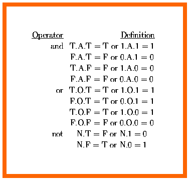
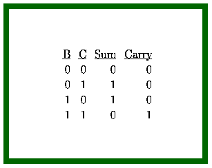
In these equations, T means true, F means false, A means "and", O means "or", N means "not." To use these operators in order to add thee two numbers we must construct a truth table of all possible outcomes.
| __B__ | __C__ | _Sum_ | Carry |
|---|---|---|---|
| 0 | 0 | 0 | 0 |
| 0 | 1 | 1 | 0 |
| 1 | 0 | 1 | 0 |
| 1 | 1 | 0 | 1 |
If your browser displays the table in an unrecognized form, click on the button to obtain the table correctly displayed in a gif picture.
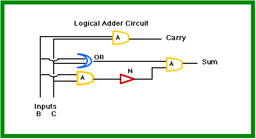
To perform this addition the following logical circuit will suffice:
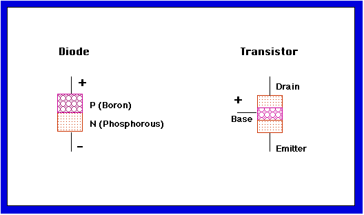
There are numerous physical ways circuits with the 0,1 property of binary numbers can be constructed: a magnet has a north and a south pole, a switch is either open or closed. The circuits could use electricity, fluids, light, or possibly even biological circuits at the atomic level. The current primary technology is electronic and employs a device called a transistor. To understand what a transistor is you must first understand what a diode is. A diode is a device which transmits a current only one way. While there are many ways of constructing diodes let us consider the silicon semiconductor technology. Consider diagram below. One block of silicon is doped with boron and the other with phosphorus. The silicon atoms are bonded together in a lattice with 8 electrons in the outer shell. Doping with phosphorus replaces some of the silicon atoms with phosphorus atoms which means there is a free electron. Doping with boron leaves the lattice one electron short creating a plus charge. Only one combination of plus and minus voltage will produce a current across the diode. If the + is attached to the p (boron) end and the - to the n (phosphorus) end the + repels the positive charges and the - repels the electrons resulting in an electron flow across the device. In the opposite case the charges in each half are attracted to the terminal and no current flows. Thus the diode possesses an asymmetric property which provides a basis for manipulating binary numbers. A transistor, which consists of two diodes placed end to end, provides an asymmetric device which amplifies the input signal. A positive voltage at the base allows current to flow from the emitter to the collector. A negative voltage at the base causes no current flow. The transistor pictured is a pnp transistor. There is also a npn transistor which is activated by a drop in voltage.
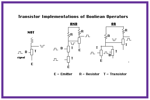
Construction of the "and", "or", and "not" using transistors. The following circuits define the "and", "or", and "not".
a. At first circuits were made with individual components wired together.
b. Later individual components were soldered into circuit boards.
c. The creation of an integrated circuit( frequently called a `chip') was motivated by the quality control problems of soldering individual electronic components into circuit boards. The development was accelerated by the competition between the US and the USSR to build smaller, more accurate guidance systems for military rockets (Military research traditionally has had deep pockets).
d. Integrated circuit technology creates electronic components directly in a silicon wafer, a thin disk of silicon cut from a circular crystal. The production procedure is to create as many 1/4" square integrated circuits as possible on the surface of the wafer. Economic incentives promote the creation of ever larger wafers. The size has increased from 2 to 8 inches.
Initially an insulating layer of silicon dioxide is deposited on the surface of the chip. The integrated circuit is then constructed with a small number of masking, etching and building steps. In the mask step the chip is first coated with photoresist. Then ultraviolet light is shone through a mask, which defines the circuit elements, on the photoresist. Where the photoresist has been exposed to the UV light it becomes soluble. In the etching step the soluble photoresist is removed with acid. This exposes portions of the underlying surface. In the building step several alternatives are possible depending on the chip design. The exposed areas could be doped with impurities to change the electrical properties of the silicon, other materials such as polysilicon, which conducts electricity could be deposited on the exposed surfaces, or the exposed areas could be etched away to create holes where aluminum is deposited.
After the integrated circuits are created on the wafer, they are tested and the good ones are packaged in plastic to protect the embedded circuits.
Once IBM began using integrated circuits to build computers, the development was market driven. Economic incentives encourage producers to crowd more and more components on each integrated circuit. If you double the number of components, the speed of an integrated circuit approximately doubles because the electronic components are closer together and smaller transistors have a shorter delay in switching. At the same time the variable production cost increases by less than two because while the details on the mask become smaller and smaller, the number of masking, etching and building steps stays constant. Nevertheless, as the number of components increase the fixed costs in the form of capital costs to build new fabrication plants increases. The empirical rate of growth of electronic components on an integrated circuit is known as Moore's Law. From 1960 to 1972 the number of components on an integrated circuit doubled each year. From 1972 to the present and perhaps until the year 2000 the number of components on an integrated circuit will double every 18 months. In l977 it was possible to place 250,000 electronic components on a integrated circuit and by the year 2000 it may be possible to place 1 billion components on a integrated circuit.
The use of electronic components has increased 2000 times from 1960 to 1977 and is still increasing. A rule of thumb is that costs fall 20 to 30%with each doubling of output. For example, the production cost of the four function electronic calculator fell from $100to $5while at the same time the general price level of all goods more than doubled. As a student, you need to distinguish between (1) the decline in cost when the number of components is doubled and (2) the decline in cost when output is doubled. For example, when technology moved from a 1M memory to the 4M memory, the number of components increased by 4, but the cost of producing 4M memory integrated circuits was less than 4 times the cost of producing 1M memory integrated circuits. When the output of 4M devices increased by 2, the cost of 4M devices fell by 20 to 30%as efficiencies in production were obtained. Consequently, the fall in cost of a bit of memory has been greater the 30%per year since 1960. This falling cost can be attributed to both cost effects.
The physical limit to the number of components per integrated circuit is temporarily limited by the resolution distance of light. Using X or Gamma rays it is physically possible to pack even more components per integrated circuit. Ultimately, the physical limit is determined by the number of atoms required to construct a circuit. But before that limit is reached the physics of ICs will shift from classical to quantum mechanics.
The economic limit is determined by the success rate in production. As more and more components are packed into the integrated circuit the failure rate goes up. One cause of such increasing failures is dust particles in the air. To reduce the possibility of contamination, integrated circuits are made in specially constructed clean rooms which filter out dust. To reduce the dust even more people are being removed from the production process through automation. Currently, and for the foreseeable future, the economic limit rather than the physical limit will control the number of components which can be placed on an integrated circuit. Achieving economic success rates as the number of components increases is why the fixed costs of creating new IC production facilities are rapidly increasing. Over time this factor will definitely slow down or even reverse the downward trend in the costs of electronic components.
There are numerous types of integrated circuits. A basic category of ICs are memory chips which are called commodity chips because they are sold in large volumes with small profit margins. The most common type of commodity chips are DRAMs, dynamic random access memory. These ICs lose all stored information when the power is turned off. At the other extreme are specialty chips which are designed for a specific purpose and produced in small lots. Intermediate are microprocessors used in PCs, communication devices, and control processes such as controlling automobile engines. Digital signal processors are used in communications.
Today worldwide commercial competition exists between US and Japanese companies. The US market was created by startup firms in Silicon Valley, CA which still excel in new product innovation. The US developed silicon compilers, which are software programs, to design custom integrated circuits automatically. Japan's strength is production efficiency of commodity integrated circuits such as memory chips. The Japanese are trying to use memory production efficiencies as the means to dominate the entire microelectronics market. To gain a strategic hold on the memory market, Japanese firms in the 80s sold memory integrated circuits below cost until most of the US firms abandoned the memory market. Japan is now leading in the production of memory chips, but now face increasing competition from Korea.
IBM, not to become a captive of the Japanese firms, creates its own memory chips. IBM has kept pace in memory chips with the Japanese. In order to improve their competitive position in relationship with the Japanese, the US has set up a research facility for improved integrated circuit production here in Austin called Semitech. Recently the US market share seems to have stabilized with respect to the Japanese. Korea has had considerable success in IC manufacturing.
The technology for making electronic ICs is also being used to make related products. Micromachines are electromechanical devices generally with moving parts such as minuscule membranes, valves, cantilevers, and bridges which can be mass-produced on silicon wafers and result in individual micromachines less than a millimeter across. Such micromachines can act as sensors for the environment or to trigger an air bag. Such devices or open or close a valve. They are being used to create inexpensive infrared cameras. There is intense international competition between the US, Japan and Europe to develop the commercial applications.
Another technology which is closely related to electronic ICs is optoelectronics which are micosemiconductor devices to process laser light and convert electricity into light or vice versa. One example is the semiconductor laser the size of a grain of sand. Other examples are encoders and decoders transferring signals from and to electricity in fiber optic communication networks. This technology is the basis for the race to build high quality, inexpensive flat TV and computer screens. In this field there is intense international competition.
If you are interested in learning more about microelectronics, check out the following:
To return to the notes remember to click `back' at the top of your screen. You may have to click several times depending how deeply you delve into these files.