Semiconductor
Manufacturing
By David Dyal 9/7/97,
11/15/97
The manufacturing of a semiconductor is an extremely sophisticated process requiring several steps with exact precision. Because of the geometry’s, or width of the chips circuits, each process must be performed with unimaginable detail.
In order to begin the manufacturing of a microchip, we must first build a foundation. This foundation is in the form of Silicon. The silicon, or glass, is extremely pure. Before device manufacturing is started, the silicon has a typical impurity concentration of less than one part per billion. The starting for virtually all semiconductor device technology is this silicon in the form of flat, circularly shaped substrates called wafers. The atoms of silicon within these wafers are arranged in a repetitive fashion on a long-range basis, and the resulting material is described as crystalline. The steps required to convert randomly ordered material into silicon wafer having long-range order is a complex procedure that is a story in itself. Silicon is one of the most abundant sources on earth representing about 25% of the earth’s crust. However, silicon combines easily with oxygen and other materials to form compounds. The silicon must first be separated from their compounds and extensively refined before it can be transformed into the single-crystal wafers used to manufacture semiconductor devices. Sand is used as the starting point for the manufacturing of silicon wafers. One the sand is refined into polycrystalline silicon, large crystals are formed which are then sliced into wafers. There are three basic steps, which are used in the preparation of silicon for use in the wafer manufacturing. The production of the polycrystalline silicon, crystal growth, and the actual manufacturing of the wafer. Through the process of heat and added chemicals such as trichlorosilane, boron, chlorides, and phosphine, pure silicon is derived and ready to be manufactured in to the silicon crystal.
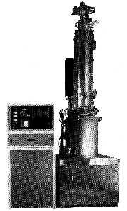
There are presently two methods used to grow single crystal silicon for semiconductor applications: the Czochralski and the float-zone crystal growth techniques. The Czochralski (CZ) method is used for about 80% to 90% of crystals grown for semiconductor use. The CZ method is by which pure polycrystalline silicon are heated to their melting point. From that point a seed crystal with the exact desired crystal structure is dipped into the molten silicon and then withdrawn at a carefully controlled rate. The process allows the molten silicon to orientate itself with the seed. As the seed is withdrawn, the molten silicon freezes in the exact replica of the seed structure. A pure silicon crystal can be grown at a rate of 2 to 4 inches per hour and is approximately three feet long when complete. There is several processes used to monitor the growth of the crystal. Crystal rotation, width, chamber atmosphere, temperature and crystal length are all critical areas of growing a successful silicon crystal.
After the crystal has been successfully grown, it must now be turned into a wafer. The first process is to grind the crystal perfectly round and determine its rotational orientation. The seed crystal has determined which crystal face will be present on the wafer surface, but the rotational position of the rod determines other axes of the crystal. Since the ingot of the silicon is one crystal, it has preferential break planes. Understanding the crystals break planes is critical later on during the device separation phase of the process. You want to make sure that the circuits are running in the same direction as the break planes so as not to destroy the chips during separation. As the crystal is being ground down, a section called the flat will identify the break direction of the crystal.
Once the crystal has been ground down, it will now be sliced into thin wafers using the flat as a reference. The blade of the saw is coated with diamond powder to enable it to cut through the hard silicon. Some challenges to overcome during the sawing process are chips, edge flakes, exit damage and wafer bowing. An etchant is used to remove saw marks and any accompanying damage from both sides of the wafer. Typically a wafer will be sent through a lapping process which is a non-abrasive machining process used to create a uniform finish on the wafer surface. Once the lapping process is complete, another etchant process is applied to remove any remaining surface deposits.
The wafer is now ready to begin the process of being manufactured into a microchip.
For more information on crystal growth, surf these sites:
|
|
The first process is the oxidation of silicon. The ability to grow a chemically stable protective layer of silicon dioxide on a silicon wafer makes silicon the most widely used semiconductor substrate. The silicon dioxide layer is both an insulating layer on the silicon surface and a preferential masking layer during the fabrication sequence.
A silicon dioxide layer is grown in an atmosphere containing either oxygen or water vapor at temperatures in the range of 900 to 1300 degrees C. Oxidation takes place when either oxygen of water vapor reacts with the silicon. The oxidation process take place in a tool called a furnace where temperatures are carefully controlled. A furnace stack or bank generally contains three to four separate furnaces, each with its own set of controls and quartzware. The furnaces elements, or coils, are heated by electrical current. The amount of electrical current is controlled and adjusted to provide the required constant temperature. A quartz tube rests inside the coils, providing an enclosure around the wafers in which the atmosphere can be controlled.
Thermal oxidation of silicon is preceded by a cleaning sequence designed to remove all contamination. Special care must be taken during this step to guarantee that the wafers do not contact any source of contamination. People in particular shed a great deal of contaminants. The cleaned wafers are dried and loaded into a quartz wafer holder called a boat. Once the boat is loaded, the wafers are ready for the oxidation process.
Thermal oxidation using dry oxygen involves controlling the flow of oxygen into the quartz tube to guarantee that an excess of oxygen is available for the silicon. A source of high purity oxygen makes sure that no unwanted impurities are incorporated in the layer of oxide as it grows. Oxygen or an oxygen – nitrogen mixture is used for growing the layer of oxide. The use of nitrogen decreases the total cost of running the oxidation process, since it is less expensive than oxygen.
The two important characteristics of a layer of silicon dioxide are its thickness and its dielectric quality. The thickness can be accurately predicted from the oxidation sequence, but it is often necessary to verify the results. The thin, uniform layers resulting from oxidation appear to have colors when observed in white light. As the oxide thickness increases from no oxide on a bare wafer to a very t hick layer, the colors observed with these thicknesses repeat themselves. To determine the thickness of a layer of oxide from its color, you need to know all of the colors preceding it on the color chart. This requirement is easily met by etching a taper in the layer of oxide by immersing the layer in hydrofluoric acid and slowly withdrawing it. The thickness can also be determined electrically by measuring the capacitance it produces between two conductive plated of a known area, or by using optical interference or physical techniques. The most commonly used instrument is a surface profilometer. A stylus with an electronically amplified output is drawn over the surface to e measured and an ink trace of the resulting profile shows the height of any step in the surface.
For more information on oxidation, surf these site:
 |
| Silicon Valley Group Inc. |
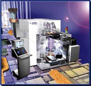
Now that there has been a completely even layer of oxide grown on the silicon surface, the next process is photolithography. Photolithography is the process step during which the geometric pattern that produces the desired electrical behavior is transformed to the surface of the wafer. The word photolithography simply means printing with light which is exactly what this process involves. The manufacture of semiconductor devices and integrated circuits consists of multiple passes through photolithography or masking as it is often called. Between photolithography, steps such as impurity reduction, oxidation or metallization will follow each masking step. The masking step defines the area where the all-future process will have their effects on the wafer. All of these processes on the wafer produce devices or circuits with specific operational behaviors.
The photolithographic process is the transfer of an image from the photomask to a wafer through the use of a photosensitive material called photoresist. Photoresist is a chemical substance containing light-sensitive mater in suspension in a solvent. The light sensitive material is selected so that it responds to the intense blue-violet light commonly in use in dark rooms or photoresist areas.
A positive or negative resist may be used in this process. Either type of resist may be used to etch the films and materials used in semiconductor manufacturing. Negative photoresist was more popular when the line widths were wider. As the line widths and spacings became smaller, the ability of positive resist to transfer smaller patterns made it more popular. 5 micrometers are typically thought of as the cross-over dimension between using positive and negative photoresist.
The photolithographic process consists of a number of steps performed sequentially, regardless or the particular photoresist being used of the layer to which it is being applied. The following is a generic definition of the Photo process sequence. First the surface of the wafer is prepared, either through the oxidation process or other types of deposition process. The photoresist is applied to the wafer either by dipping the wafer in the solvent, spraying the wafer or spinning the resist onto the wafer surface. The wafer is then soft baked
to remove any excess solvent. Soft baking is typically done in convection heating. This is a process by which a current of hot filtered air or dry nitrogen circulates through an oven set at a constant temperature, evaporating the solvent.
After the wafers have been cooled, they are ready to be aligned and exposed. The mask, or circuit pattern, and the wafer are positioned in a precise manner in respect to each other. The alignment process is made possible by using highly sophisticated optics and controls for positioning both the wafer and the mask. Once the mask and wafer are in place, the mask pattern is exposed to the surface of the wafer. Once this is exposure is complete, the mask moves on to the next part of the wafer to expose this pattern of circuits again and again until the entire wafer area requiring this pattern is complete. When a wafer is made, assume that on a wafer six inches in diameter has about 150 chips. Each chip is about the size of you pinky fingernail. During the photolithography process, it is not just one exposure per layer of circuit pattern. It is, in fact, exposed for each chip on each layer. You therefore have a particular mask that will be exposed up to 150 times per layer. One exposure per each chip on each layer of the wafer. There can be up to 18 layers of circuits on each individual chip. Each circuit layer is placed on the wafer by exposing and developing the mask.
Following the exposure process, those photoresist regions with the highest solubility are dissolved which develops the pattern of the mask. Development can be performed by either dipping the wafer in the developer or spraying developer onto the wafer surface. The wafer is then inspected to determine the accuracy of the first image transfer process. Inspection can be completed either manually or automatically. All wafers that do not pass inspection are removed from the lot and sent back for rework.
For more information on Development, surf this site:
 |
| FSI International |
Hard-bake is the next step in photolithography. The purpose of hard-bake is to evaporate any solvents left in the resist layer following development and to increase adhesion at the edges of the photoresist pattern. Hard-bake is the same as soft bake but with higher temperatures.
Etch is a process by which material is removed from regions that are not protected by photoresist, but does not attack the photoresist. Etchants have the ability to remove material both vertically and horizontally. Isotropic etches the same in all directions where as anisotropic etches more rapidly in one direction than in another. These different etchants are used to create different characteristics on the wafer.
Liquid etching or wet etch is accomplished by dipping the wafers in an etching solution at a particular temperature. Some chemicals used in wet etch are phosphoric acid, nitric acid or buffered oxide etch. Once the unprotected areas are etched, the wafer is ready to have the resist stripped. Once it has been determined that the etch process has bee successful, the wafer is then dipped in deionized water to halt any further etch reactions.
Dry etch has become the more popular etch process because of the smaller line-widths and spaces. Dry etch allows the process engineers to have much greater control as to the amount of material that is being etched away from the wafer. The three main types of dry etch are plasma etch, reactive etch and physical etch.
Plasma etch is when wafers masked with photoresist are placed in a chamber which is evacuated. A small amount of reactive gas is introduced into the process chamber. At that point, an electromagnetic field is then applied and the layer that is not protected by the photoresist is etched away by the etchant gas.
Reactive etching is a technique that is a combination of physical and chemical etching. It combines controlled energetic ion bombardment with chemically reactive interaction.
Physical etching is the use of energetic particles to physically remove material. A beam of charged particles is used in the technique called ion milling. Ion milling is similar to reactive ion etching, except that it uses only the energy of motion of the ions to etch material.
Once the etch process has been completed, strip resist is the next process step in photolithography. The strip resist process removes the layer of photoresist from the wafer without creating any damage. As with etching, bot a wet or dry process may be utilized. Chemicals in the wet process such as hydrogen peroxide, sulfuric acid or ammonium persulfate are used to strip the remaining resist.
For more information on etch, surf these sites:
 |
Final inspection is the final operation in photolithography. Each wafer is examined closely using an optical microscope. Wafers that do not meet certain standards are sent back for reprocessing of are removed from the line completely. All good wafers are sent on for subsequent processing.
In summary of the photolithographic process in manufacturing integrated circuits, there are eleven steps to complete the entire process. While a wafer is being processed, these eleven steps account for only a partial layer of the chip. The one layer of the wafer is still not complete. As you will read, there are several more processes in manufacturing the first layer of the chip before going back to repeat all these steps to build on to achieve the chips operational goals.
For more information on Photolithography, surf to:
 |
This next section will be more involved with the characteristics involved in carrying electrical signals through the silicon and how devices are created to form the integrated circuits.
To start with, properties called impurities are introduced into the silicon wafer. Two ways to introduce these impurities are through thermal predeposition and ion implantation. The intent of the process is to generate dopant atoms in specific regions of the wafer. These doped areas become the transistors, diodes and other devices that make up the integrated circuit.
Diffusion is the process whereby particles move from regions of higher concentration to regions with lower concentration. Imagine putting a drop of black ink into a glass of water. Gradually the ink moves from the ink drop throughout the entire glass of water. During this process, the water on the top is very dark and the water on the bottom is clear with a graduation of colors in between. As time passes, the ink spreads out until it is possible to see through it, though some areas are darker than others. Finally, a steady state is reached and the ink is uniformly distributed in the water. The movement of ink from the region of high concentration to the region of low concentration is an illustration of the process of diffusion.
Diffusion is used to introduce controlled amounts of chosen impurities into selected areas of a semiconductor crystal. The most common way of getting impurities into the silicon is through predeposition. During predeposition, the semiconductor substrates are heated to a selected and controlled temperature and an excess amount of desired dopant is made available in the process chamber. The materials used as dopants enter the crystal structure until a maximum concentration is reached. The maximum concentration called solid solubility of a wafer depends on the temperature of the wafer and only temperature. The hotter the wafer, the more dopants will be absorbed into the silicon crystals. Time and heat are the two playing factors for a wafer to reach solid solubility.
In the fabrication of the silicon devices, the presence or absence of a layer of silicon dioxide on the surface of the wafer determines where the dopant is allowed to enter the silicon. As long as a silicon dioxide layer of sufficient thickness is used, predeposition will introduce dopants only in the desired area. This will allow the process engineers to place diodes, transistors and other devices in areas where needed on the integrated circuit. Predeposition in this manner is performed in the same furnaces that are used to grow the silicon dioxide layer on the pure silicon. These are called diffusion furnaces and run at incredibly high temperatures. Temperatures in these furnace tubes typically run between 900 and 1300 degrees Celsius. Some of the gases that are used for dopants are silane, boron trichloride and phosphine, through there are several other types of gases and chemicals used in this process. Which gases or chemicals that are used is determined by what type of circuit you are making and out of what type of material the wafer is made.
One other popular way of introducing dopants into semiconductors is through ion implantation. This process selects ions of desired dopants, accelerates them using an electric field and scans them across a wafer to obtain a uniform predeposition. The energy imparted to the dopant ion determines the ion implantation depth.
Once the doping species of gas has been determined, (usually boron, phosphine and arsine), the two variables that are controlled are the number of ions that reach the wafer per unit of area and the energy with which they reach the wafer. The dose of ions is controlled by counting the ions as they pass a detector, and the energy is controlled by changing the voltage along the acceleration chamber. In order to control where the ions end up on the wafer is determined by either using a patterned layer of material such as silicon dioxide of photoresist as a mask. Following implantation and any subsequent cleaning steps, the implanted wafers are often put through a high temperature furnace to activate any ions that may not have come to rest in electrically active locations in the crystal structure.
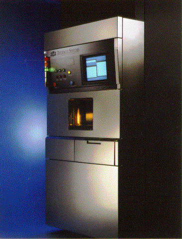
Following Ion Implantation come the process of epitaxial deposition. Epitaxial deposition is the deposition of a single crystal layer on a substrate such that the crystal structure of the layer is an extension of the crystal structure of the substrate.
For more information on ion implanting, surf:
 |
In the manufacturing of silicon diodes and transistors, devices with higher switching speeds, breakdown voltage or current handling capability are obtained by using epitaxial deposition. In diode fabrication, a heavily doped silicon substrate used as the starting material results in a diode with lower resistance to current flow. However, high doping concentrations produce lower reverse junction breakdown, so an epitaxial layer of lightly doped silicon of the same conductivity type is deposited on the substrate for the actual fabrication of the junction.
Transistors are fabricated in a manner using an epitaxial layer for the lightly doped collector region and diffusing in a base and an emitter. The epitaxial layer may also be of the opposite conductivity type, in which case, it serves as the base of the transistor, and the emitter is added during subsequent high temperature diffusion.
This epitaxial layer on the substrate helps provide electrical isolation between devices in adjacent pockets when the circuit is in operation. It also provides a crystal layer allowing for the process of additional layers of circuits on the substrate without having to go down into the substrate itself. Depending on the type of circuit you are manufacturing, the epitaxial layer can either be made up of positive or negative electron charges within the crystal layer. Typically, the epitaxial layer matches that of the substrate layer crystal structure and characteristics.
For more information on Epitaxy, surf these sites:
|
 |
Now that all of the devices such as diodes, transistors and junctions have been manufactured on the chip, they must be connected together to perform circuit functions. The connection process is called metallization and is performed using one of several methods. In order to serve as an excellent interconnects, the metal must meet the following requirements. It must make a low resistance electrical contact with the silicon. The metal must have the limited reactivity with silicon in order to produce a stable contact. It must have a high electrical conductivity so that high current is easily carried without any voltage drops. The metal must adhere well to the underlying silicon, silicon dioxide or other dielectric used. The metal must cover different levels in the surface topography. It can not corrode under normal conditions. The metal must bond easily to the metallization to allow for external connections and finally the metal must be economically competitive.
Though no metal meets all of these requirements, aluminum is the metal that most closely matches these requirements. In order to increase the ability of aluminum for this application, impurities such as small amounts of silicon are added during the deposition phase to decrease its reaction to silicon. Similarly, copper is added to enhance it conductivity capabilities.
A metal layer on the wafer is most often obtained by using a vacuum deposition technique. This means that the process chamber must be evacuated to provide a sufficient vacuum for the deposition to take place. A vacuum pump must reduce the gas pressure in the chamber to an acceptable level. Instruments need to monitor the vacuum level and other system parameters and a method of depositing the desired layer of material must all be achieved to get the desired results in laying this layer (s) of metal.
There are four techniques used in laying a layer of metal. They are:
Filament evaporation; A current flows through a filament causing first melting and then evaporation of the material filament.
Electron-beam evaporation; An intense beam of electrons is used to evaporate the material on contact.
Flash evaporation; A wire of pellets is fed onto a hot ceramic substrate, evaporating the material on contact.
Sputtering; A gas at low pressure, such as argon, bombards and dislodges atoms from a target of the material to be deposited.
Filament evaporation is the simplest and most economical process. Evaporation is accomplished by gradually increasing the current flowing through a filament to first melt the loops of material on the filament, thereby wetting the filament. Once the filament is wetted, the current through it is increased to accomplish the evaporation.
Electron-beam evaporation uses a focused beam of electrons to heat the material. A high intensity beam of electrons is generated in a manner similar to that used in a television picture. The focused beam of electrons melts the material contained in a hearth, a water-cooled block with a large depression for holding the evaporation source. Only electrons come in contact with the material to be evaporated, so it can be a low contamination process.
Flash evaporation is similar to filament evaporation in that the material is evaporated by thermal resistance heating, but that is the only similarity. Flash evaporation uses a continuously fed spool of wire incident on the heated ceramic bar for deposition. This deposition technique combines the speed and the contamination-free features of E-beam deposition with the radiation-free feature of a filament evaporation.
In the sputtering method, ions of an inert gas such as argon are introduced into the chamber after a satisfactory vacuum level has been reached. An electric field ionizes these atoms and accelerates them toward one electrode in the chamber, called the target. When the ions strike the target, the dislodge atoms from it, depositing them on the substrate facing the target.
No matter which process you use the following steps are;
Clean the wafers and remove all contamination and dry the wafer. Position the wafer in the vacuum chamber so that they will receive a uniform layer. Close the vacuum chamber and pump the chamber down. Close the valve to the roughing pump, and open the valve to the high vacuum pump. Allow the system to reach a low vacuum level. Turn on the source and evaporate a small amount of material onto a shield between the source and the wafers to clean the source. Deposit the necessary thickness of the material on the substrates. Turn the source off and cool the wafers and the chamber. Fill the chamber with an inert gas, open the chamber and remove the wafers.
The wafer is now ready finished and must go to packaging. Packaging is as important as any other step in the process. First a wafer goes through back-side lapping. This is a process that removes any diffused layers that may interfere with the wafers electrical properties, to make is easier to separate the die or to prepare the backside for other metal deposition processes. Back-side metal deposition is a process where gold is deposited on the wafers back to make the attachment of the separated die (chip) to the package easier in the later operations.
For more information on testing and packaging, surf this site:
| Minco Technology Labs |  |
One, both or none of these steps need to take place before moving on to final process. These previous two steps may occur depending on the devices being processes.
Wafer sort is when the wafers are placed on a wafer prober and the individual die on each wafer is tested. Pointed metal probes contact each bonding pad and supply the necessary current and voltages to the device. Those devices that function properly are left alone while those that fail are marked with a drop of ink.
Now comes the process of separating the devices on the wafer. First the wafer is scribed with either a laser scribe or a diamond scribe. The wafer is then bent and breaks on these scribes. A more recent development is using a diamond saw to cut the wafer apart to separate the devices.
For the convenience of handling, the good die are attached to a package or a leadframe. Four types of die-attach are encountered Eutectic die attach involves the prior deposition of a layer of metal, such as gold to the wafers backside. By heating the package to a certain temperature and placing the die on it, a bond is formed between the die and the package. Preform die-attach involves the use of a small piece of material of special composition that will adhere to both the die and the package. A preform is placed on the die-attach area of a package and allowed to melt. The die is then scrubbed across the region until is attached, and then the package is cooled. Soft solder die-attach uses a metal, such as silver deposited on the backside of the wafer to form the bond. A lead-tin preform melts at the die-attach temperature, bonding the package to the die. Epoxy die-attach involves the use of an epoxy glue to attach the die to the package. A drop of epoxy is dispensed on the package and the die is placed on top of it. The package may need to be baked at an elevated temperature to cure the epoxy properly.
Wire bonding is when a wire is used to electronically connect the bonding pads of the device to the package. Either gold or aluminum is used in this process. Three methods of attaching the wires between the device pads and the package are thermo-compression, ultrasonic and thermosonic bonding. Thermo-compression bonding is used with gold wire and involves heating the package and forming the bond between the wire and the pad using both heat and pressure. Ultrasonic bonding uses a pulse of ultrasonic energy to provide a scrubbing action that forms a bond between the aluminum wire used and the pad. Thermosonic bonding uses gold wire and a combination of heat and a pulse of ultrasonic energy.
Once a device is packaged, it is ready for final testing. This testing is the same as the test the die went through at wafer sort. During packaging, some damage to the die may occur, therefore, it must go through wafer probe once again to ensure its functionality.
The device is now ready to sell.
For further information on semiconductor suppliers, manufacturers:

For semiconductor industry standards:

