![]()
![]()
![]()
Next: Hardware
Software and Up:Info: Info Society Previous: Binary Numbers
Objective: In the last lecture we discussed the use of binary numbers to represent numbers, letters, mathematical symbols, voice, and pictures. This lecture covers the current technology for manipulating the strings of binary numbers, microelectronics. Future manipulation of strings of binary numbers may be based on light circuits. The index for this section is:
In the 19th century George Boole invented Boolean algebra as
a theoretical study. In the 20th century, Boolean algebra
has become the basis for designing circuits to manipulate binary
numbers. Because the 0,1 of binary numbers can be represented by true
(1) and false (0), circuits can be analyzed by Boolean algebra. This
is very important because the analysis of a circuit can be independent
of how it is realized by a specific technology. Currently, the
prevalent integrated circuit technology is electric circuits
embedded in 1/4" squares of silicon known as chips. (Digression on
vocabulary: In your readings you will find some writers use the term
chip for the integrated circuit, not just the 1/4" square of silicon on
which the circuit is embedded.) Someday the technology could switch to
laser light in light circuits. The presently designed Boolean circuits
could be realized in the new technology without necessitating a
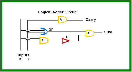
redesign. To gain an idea of how Boolean algebra might be employed, let
us consider how we might add two numbers, B and C, where each number
can take on values of 0 or 1. It turns out that all arithmetic
operations can be performed using three Boolean operators,
which are "and","or", and " not".
|
Operator |
Definition |
|---|---|
|
|
|
|
|
|
|
|
|
|
|
|
|
|
|
|
|
|
|
|
|
|
|
|
|
|
|
|
|
|
__B__ |
__C__ |
_Sum_ |
Carry |
|---|---|---|---|
|
|
|
|
|
|
|
|
|
|
|
|
|
|
|
|
|
|
|
|
There are numerous physical ways that circuits with the 0,1 property
of binary numbers can be constructed: a magnet has a north and a south
pole, a switch is either open or closed. The circuits could use
electricity, fluids, light, or possibly even biological circuits at the
atomic level. The current primary technology is electronic and employs
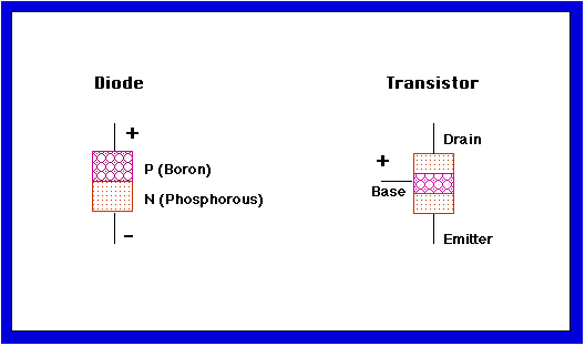
a device called a transistor. To understand what a transistor
is, you must first understand what a diode is. A diode is a
device which transmits a current only one way. While there are many
ways of constructing diodes, let us consider the silicon semiconductor
technology. Consider the diagram below. One block of silicon is doped
with boron and the other with phosphorus. The silicon atoms are bonded
together in a lattice with 8 electrons in the outer shell. Doping with
phosphorus replaces some of the silicon atoms with phosphorus atoms
which means there is a free electron. Doping with boron leaves the
lattice one electron short creating a plus charge. Only one combination
of plus and minus voltage will produce a current across the diode. If
the + is attached to the p (boron) end and the - to the n (phosphorus)
end, the + repels the positive charges and the - repels the electrons
resulting in an electron flow across the device. In the opposite case
the charges in each half are attracted to the terminal and no current
flows. Thus the diode possesses an asymmetric property which provides a
basis for manipulating binary numbers. A transistor, which consists of
two diodes placed end to end, provides an asymmetric device which
amplifies the input signal. A positive voltage at the base allows
current to flow from the emitter to the collector. A negative voltage
at the base causes no current flow. The transistor pictured is a pnp
transistor. There is also a npn transistor which is activated by a drop
in voltage.
Click here for a more complete explanation of a transistor.
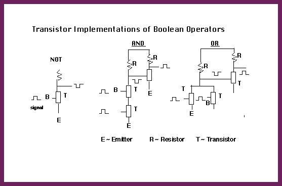
Construction of the "and", "or", and "not" using transistors. The
following circuits define the "and", "or", and "not".
a. At first circuits were made with individual components wired
together.
b. Later, individual components were soldered into circuit boards.
c. The creation of an integrated circuit( frequently called a `chip')
was motivated by the quality control problems of soldering individual
electronic components into circuit boards. The development was
accelerated by the competition between the US and the USSR to build
smaller, more accurate guidance systems for military rockets (military
research traditionally has had deep pockets).
d. Integrated circuit technology creates electronic components directly
in a silicon wafer, a thin disk of silicon cut from a circular crystal.
The production procedure is to create as many 1/4" square integrated
circuits as possible on the surface of the wafer. Economic incentives
promote the creation of ever larger wafers. The size has increased from
2 to 8 inches.
Initially an insulating layer of silicon dioxide is deposited on the
surface of the chip. The integrated circuit is then constructed with a
small number of masking, etching and building steps. In the mask step
the chip is first coated with photoresist. Then ultraviolet light is
shone through a mask, which defines the circuit elements, on the
photoresist. Where the photoresist has been exposed to the UV light it
becomes soluble. In the etching step the soluble photoresist is removed
with acid. This exposes portions of the underlying surface. In the
building step several alternatives are possible depending on the chip
design. The exposed areas could be doped with impurities to change the
electrical properties of the silicon, other materials such as
polysilicon, which conducts electricity could be deposited on the
exposed surfaces, or the exposed areas could be etched away to create
holes where aluminum is deposited.
After the integrated circuits are created on the wafer, they are tested
and the good ones are packaged in plastic to protect the embedded
circuits.
Integrated Circuits:
Once IBM began using integrated circuits to build computers, the
development was market driven. Economic incentives encourage producers
to crowd more and more components on each integrated circuit. If you
double the number of components, the speed of an integrated circuit
approximately doubles because the electronic components are closer
together and smaller transistors have a shorter delay in switching. At
the same time the variable production cost increases by less than two
because while the details on the mask become smaller and smaller, the
number of masking, etching and building steps stays constant.
Nevertheless, as the number of components increases, the fixed costs in
the form of capital costs to build new fabrication plants increases.
The empirical rate of growth of electronic components on an integrated
circuit is known as Moore's Law. From 1960 to 1972 the number
of components on an integrated circuit doubled each year. From 1972 to
the present and perhaps until the year 2000 the number of components on
an integrated circuit will double every 18 months. In l977 it was
possible to place 250,000 electronic components on an integrated
circuit and by the year 2000 it may be possible to place 1 billion
components on an integrated circuit.
The use of electronic components has increased 2000 times from 1960 to
1977 and is still increasing. A rule of thumb is that costs fall 20 to
30%with each doubling of output. For example, the production cost of
the four-function electronic calculator fell from $100 to $5 while at
the same time, the general price level of all goods more than doubled.
As a student, you need to distinguish between (1) the decline in cost
when the number of components is doubled and (2) the decline in cost
when output is doubled. For example, when technology moved from a 1M
memory to the 4M memory, the number of components increased by 4, but
the cost of producing 4M memory integrated circuits was less than 4
times the cost of producing 1M memory integrated circuits. When the
output of 4M devices increased by 2, the cost of 4M devices fell by 20
to 30% as efficiencies in production were obtained. Consequently, the
fall in cost of a bit of memory has been greater than 30% per year
since 1960. This falling cost can be attributed to both cost effects.
The physical limit to the number of components per integrated circuit
is temporarily limited by the resolution distance of light. Using X or
Gamma rays it is physically possible to pack even more components per
integrated circuit. Ultimately, the physical limit is determined by the
number of atoms required to construct a circuit. But before that limit
is reached the physics of ICs will shift from classical to quantum
mechanics.
The economic limit is determined by the success rate in production. As
more and more components are packed into the integrated circuit the
failure rate goes up. One cause of such increasing failures is dust
particles in the air. To reduce the possibility of contamination,
integrated circuits are made in specially constructed clean rooms which
filter out dust. To reduce the dust even more, people are being removed
from the production process through automation. Currently, and for the
foreseeable future, the economic limit rather than the physical limit
will control the number of components which can be placed on an
integrated circuit. Achieving economic success rates as the number of
components increases is why the fixed costs of creating new IC
production facilities are rapidly increasing. Over time this factor
will definitely slow down or even reverse the downward trend in the
costs of electronic components.
Two other economic factors in IC design and production are the fixed cost of building a production foundry and the amount of heat generated by ICs. As the number of components on an IC has increased so has the construction cost of a new production facility. Now the cost is billions of dollars so that even major players now sometimes construct such facilities as joint ventures. The amount of heat generated by ICs has also rapidly increased with increasing numbers of components. A 2Bhz pentium 4 generates 70 watts of heat and a supercomputer as much as 5000 watts. Cooling computers is becoming a major problem. Designers are searching for ways to reduce heat production of ICs.
The end of Moore's law may occur in the second decade of the 21st century when IC makers hit insurmountable barriers and have to shift to quantum mechanics ICs, nanotubes, or building ICs atom by atom-Nanotechnology. Progress will probably continue with combinations of new approaches with current IC technology.
Moore's Law
Today worldwide commercial competition exists between US, Japanese,
Korean, and European companies and this competition among firms is what
made Moores Law an empirical fact . The US market was created by
Silicon Valley, CA startup firms, which still excel in new product
innovation. The US developed silicon compilers, which are software
programs, to design custom integrated circuits automatically. Japan's
strength is production efficiency of commodity integrated circuits such
as memory chips. The Japanese tried to use memory production
efficiencies as the means to dominate the entire microelectronics
market. To gain a strategic hold on the memory market, Japanese firms
in the 80s sold memory integrated circuits below cost until most of all
but two US firms abandoned the memory market. IBM, not to become a
captive of the Japanese firms, creates its own memory chips. IBM has
kept pace in memory chips with the Japanese. Japan gained the lead in
IC production.
To compete a firm must simultaneously crowd more and more electronic
components into a chip and at the same time constantly improve the
efficiency of the production process. In order to improve their
competitive position in relationship with the Japanese, the US set up a
research facility for improved integrated circuit production here in
Austin called Sematech. The
production efficiency of ICs is dependent on the size of the wafer on
which ICs are made. The bigger the wafer the more efficient the
process. Competition has created incentives for shifting production to
larger and larger wafers. US and Korea got back into the game when
Japanese firms hesitated in investing in the 300mm wafer size. The IC
indusry has now moved to 300mm waferss and the US firms concentrated
their research efforts in more profitable types of ICs such as
microprocessors, communication ICs and specialty ICs. Recently the US
electronics industry has regained the worldwide lead in
microelectronics sales and now Samsung of South Korea is the number one
manufacturer of memory chips.
There are numerous types of integrated circuits. A basic category of ICs are memory chips which are called commodity chips because they are sold in large volumes with small profit margins. The most common type of commodity chips are DRAMs, dynamic random access memory. These memory chips do not hold their memory when power is turned off. An increasingly important type of memory chip is Flash memory that maintains its memory when power is turned off.
Microprocessors used in PCs, communication devices, and control
processes such as controlling automobile engines, appliances, or smart
cards are produced in intermediate volumes.
At the other extreme are specialty chips which are designed for a
specific purpose and produced in small lots.
Microelectronics
MEMS technology is Micro-Electonic-Mechanical Systems that extends ICs by integrating other types of components such as mechanical components. Two examples here are presure sensors and accelerometers. An example of the latter is the MEMS device to activate an air bag in a car. MEMS devices can also include RF (radio frequency) circiuts and with technological advances should improve communications in general. For example, RFID or radio frequency identification tages are now replacing bar codes for inventory and other identification tasks. Another new type of sensor has the name Smart Dust because these sensors are so small that they can float in space and communicate back their measurements. These sensors will be especially useful in dangerous situations such as the military, nuclear and other industrial accidents, and police work.
MEMS Technology
An example of complining MEMS with chemical sensors is Sandia Labs research in creating sensors to detect enviromental degradation.
Recently progress has been made right here at UT in taste. The E-tongue has arrays of pyramidal pits filled with plastic beads that hold chemical receptors in an IC:
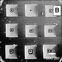
The chemical receptors turn different colors when exposed to liquid and solid food. The taste is recorded by recording the light patterns in a special camera. Once this technology is perfected the E-tongue could be fitted with a very large number of different type of receptors to create a much more sensitive tongue than the human tongue. For a second electronic is the ASTREE electronic tongue
In the food and beverage industry such E-tongues will be used to compare tests of products with libraries of previously tasted products. The E-tongue will also be used in medical diagnosis to screen blood and urine samples to taste for such chemicals as cholesterol or cocaine. It can also be used to detect toxins in water. A Swedish dairy uses an e-tongue to speed up production.
Chemical and Taste
There are several competing technologies for the E-nose. We will present the E-nose being developed by Nordic Sensor Technologies. A schematic of their E-nose is:
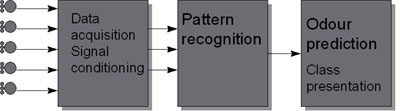
Where E-noses differ is the technology to detect various types of gas molecules. Where they are similar is that most require a neural network program to recognize the type of order present.
Nordic Sensor Technologies uses ten MOSFET gas sensors. Over time the number and types of gas sensors is almost certainly likely to grow. By using specialized groups of gas sensors, E-noses can be used in specific tasks.
Some uses of E-noses are:
Affymetrix and Stanford have developed an IC that can perform DNA analysis. These ICs combine IC technology with application-specific oligonucleotide arrays. The nucleic acid to be analyzed is amplified and labeled with a fluorescent marker. The labeled target is then exposed to the detection IC. The positions where the detection IC is fluorescent tell through complimentarity the DNA sequences of the target. This technology will probably have an explosive growth in the 21st century. Research in bio chips is taking place at many institutions:
As I understand the limits of nanotechnolgy there are two branches. One is the creating compound by manipulating materials at the molecular level such as coatings and paints. Some of these products may be super toxic. The other is the creation of machines at the molecular level such as integrated circuits. This is a hot research area that is now the first branch is entering the commercialization period.
Another technology, which is closely related to electronic ICs, is optoelectronics that are microsemiconductor devices to process laser light and convert electricity into light or vice versa. With fiber optics becomming the most important technology for communication this is a vast area of applications. Another area is production of electricity for sunlight using solar cells. One example is the semiconductor laser the size of a grain of sand. Other examples are encoders and decoders transferring signals from and to electricity in fiber optic communication networks. This technology is the basis for the race to build high quality, inexpensive flat TV and computer screens. In this field there is intense international competition.
Light
![]()
![]()
![]()
Next: Hardware
and Software Up:Info: Info Society Previous: Binary Numbers